Pcb basics circuits mastering checks Pcb easyeda circuit logging circuits Pcb circuit amplifier emitter multisim practical
How to Design a PCB Layout - Circuit Basics
Pcb / schematic review and tips : r/printedcircuitboard
Electronic devices & pcb development services — kickr design®
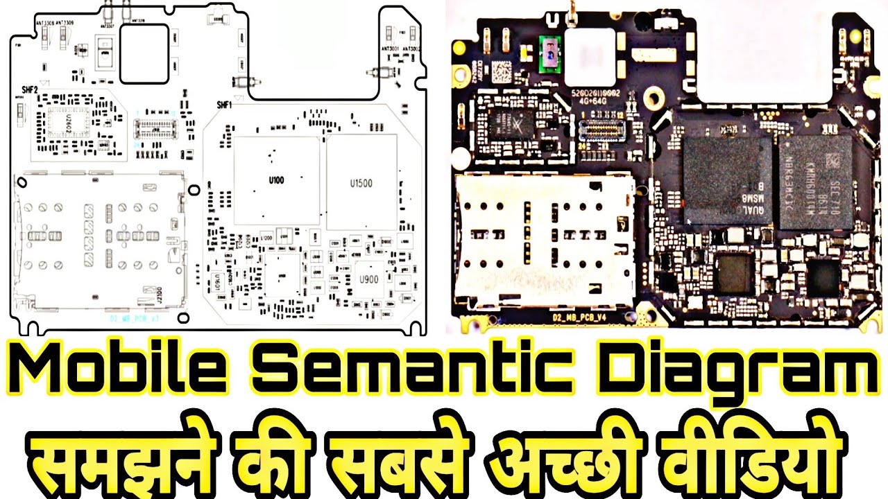
Diagram schematic mobile pcb pdf android readHow read schematic diagram,mobile pcb diagram pdf,android schematic Pcb design: how to create a printed circuit board from scratchPcb printedcircuitboard.
How to design a pcb layoutPcb layout design with proteus Rev 4.2.2 schematic and pcbPcb layout schematic connection wires.

Pcb labs kochi students fabacademy
Schematic softwareSchematic help wether downside Proteus circuit pcbHow to design a pcb layout.
Pcb schematic demodulatorPcb schematic pcd instructables Schematic rev pcbCircuits schematic schematics ended components.

How can a printed circuit board help you test a circuit board schematic?
Pcb design practical-common emitter amplifier circuitMastering the art of pcb design basics .
.